Solid Copper vs. Hatched Copper in Flex PCB
- Flex Plus Tech team
- Mar 13
- 2 min read
Updated: Mar 31
In flexible PCB design, the choice of copper fill significantly impacts electrical performance, durability, and electromagnetic interference (EMI) shielding. The two most common copper fill methods are Solid Copper and Hatched Copper. But what are the differences, and which one is best for your application? This article will compare the two approaches to help you make an informed decision.
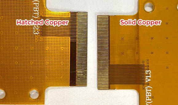
What is Solid Copper?
Superior Conductivity & EMI Shielding: Solid copper fill means a continuous copper layer without gaps, offering excellent conductivity and shielding properties.
Advantage
Excellent Conductivity – Ideal for high-power applications as it can carry larger currents.
Strong EMI Shielding – Reduces electromagnetic interference, making it suitable for high-frequency circuits.
Better Heat Dissipation – A continuous copper layer helps distribute heat evenly, preventing overheating.
Disadvantages
Limited Flexibility – More prone to cracking when bent due to the rigid copper layer.
Higher Manufacturing Difficulty – Uneven etching can occur, increasing production complexity.
Slightly Heavier–Might add unnecessary weight in lightweight applications.
Best Use Cases for Solid Copper
High-current applications (e.g., power layers, high-power circuits)
High-frequency devices requiring strong EMI shielding (e.g., RF circuits, wireless communication)
Applications needing better heat dissipation.
What is Hatched Copper?
Enhanced Flexibility for Lightweight Designs: Hatched copper uses a grid-like structure instead of a solid layer, balancing conductivity with flexibility.
Advantages of Hatched Copper
Greater Flexibility – Reduces stress concentration, preventing copper cracks in bending areas.
Easier Manufacturing – Reduces etching-related stress, making production more stable.
Lightweight – The copper fill rate ranges from 30% to 70%, with line widths of 0.1-0.3mm. making the PCB thinner and lighter.
Disadvantages of Hatched Copper
Lower Conductivit - Higher resistance compared to solid copper, making it less suitable for high-current applications.
Weaker EMI Shielding – Grid gaps may allow electromagnetic interference, making it unsuitable for high-frequency circuits.
Less Effective Heat Dissipation – The grid structure reduces the copper surface area, limiting thermal conductivity.
Best Use Cases for Hatched Copper
Highly flexible applications (e.g., wearable devices, foldable displays)
Low-power, low-current circuits (e.g., sensors, touch panels)
Lightweight electronic devices (e.g., aerospace, medical electronics)

Solid Copper vs. Hatched Copper: Which One Should You Choose?
If your flexible circuit board needs to carry high currents or requires strong EMI shielding, solid copper is the best option.
If your flexible circuit board needs to bend frequently or is used in lightweight, low-power applications, hatched copper is the better choice.
For optimal results, consider hybrid designs–using solid copper in high-current areas and hatched copper in flexible sections.
Conclusion: Optimizing Flex PCB Design
When designing your flexible printed circuit boards, consider signal integrity, current capacity, bending durability, and cost to select the best copper fill method. A well-optimized PCB will enhance product longevity and efficiency.
Stay Updated with More PCB Design Tips!
We hope this article clarifies the differences between solid and hatched copper in flex PCB boards. If you have any questions about flex PCB design, feel free to leave a comment!
Kommentare