Flex PCB Fabrication: Additive and Subtractive
- Flex Plus Tech team

- Dec 30, 2024
- 3 min read
Updated: May 11
Exploring the Core Techniques in Flex PCB Fabrication
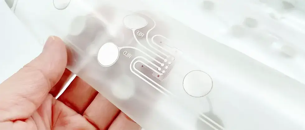
The evolution of modern electronics has been profoundly shaped by advancements in printed circuit board technology. Among these innovations, flex PCB fabrication stands out as a critical enabler of compact, lightweight, and durable devices. Flex circuits are designed to bend and conform to dynamic mechanical environments, making them indispensable in applications ranging from camera systems to humanoid robot technology. At the heart of flex PCB manufacturing lie two fundamental methodologies: additive and subtractive processes. This article delves into the intricacies of these techniques, their advantages, limitations, and their roles in shaping the future of flex PCB fabrication.
Flex PCB Fabrication: An Overview
Flex PCB Fabrication involves creating circuits on flexible substrates, typically polyimide or polyester films. Unlike rigid PCBs, flex circuits require specialized manufacturing methods to ensure reliability under repeated bending and environmental stress. The choice between additive and subtractive methods depends on design complexity, material efficiency, and cost considerations.
Key Components of Flex PCBs
Substrate: PI is the most common base material due to its thermal stability and flexibility.
Conductive Layers: Copper is the main conductor, applied via electroplating or lamination.
Adhesives and Coverlays: Protect circuits and enhance mechanical durability.
Stiffeners: Reinforce areas requiring rigidity, such as connector mounts.
Additive Manufacturing in Flex PCB Fabrication
The additive method forms conductive traces by selectively depositing material onto the substrate. This method minimizes waste and is ideal for high-precision, low-volume production.
Process Steps in Additive Fabrication
Substrate Preparation: Clean and treat the polyimide film to ensure adhesion.
Seed Layer Deposition: Apply a thin conductive layer to serve as a foundation.
Photoresist Application: Coat the substrate with a light-sensitive polymer.
Exposure and Development: Use UV light to pattern the photoresist, exposing areas where copper will be deposited.
Electrochemical Deposition: Copper is deposited onto the exposed seed layer through electrolysis to form conductive traces.
Etching and Finalization: Strip the remaining photoresist and clean or finish the surface as required.
Advantages of Additive Methods
Material Efficiency: Reduces copper waste by up to 70% compared to subtractive techniques.
Fine Feature Resolution: Achieves trace widths below 25 µm, critical for high-density interconnects.
Design Flexibility: Supports complex geometries and multilayer stacking.
Limitations
Higher Initial Costs: Requires expensive equipment for seed layer deposition.
Slower Throughput: Not ideal for mass production.
Subtractive Manufacturing in Flex PCB Fabrication
The subtractive method starts with a fully copper-clad substrate and removes unwanted material to form circuits. This traditional approach dominates high-volume production due to its scalability.

Process Steps in Subtractive Fabrication
Lamination: Bond copper foil to the polyimide substrate using heat and adhesive.
Photoresist Coating: Apply a dry film or liquid photoresist.
Patterning: Use UV light to pattern the photoresist, revealing the seed layer areas where copper will be subsequently deposited
Etching: Immerse the board in a chemical solution (e.g., ammonium persulfate) to dissolve exposed copper.
Stripping and Finishing: Remove the photoresist and apply surface finishes (e.g., ENIG or OSP ).
Advantages of Subtractive Methods
Cost-Effectiveness: Lower per-unit costs for large batches.
Proven Reliability: Mature technology with standardized processes.
Faster Turnaround: Suitable for high-volume orders.
Limitations
Material Waste: Up to 80% of copper is etched away.
Limited Resolution: Trace widths typically exceed 50 µm.
Comparing Additive and Subtractive Methods
Choosing between additive and subtractive techniques hinges on project requirements:
Factor | Additive | Subtractive |
Material Efficiency | High (minimal waste) | Low (significant waste) |
Precision | <25 µm traces | >50 µm traces |
Cost Structure | High upfront, low marginal | Low upfront, high marginal |
Production Volume | Low to medium | High |
Environmental Impact | Lower chemical usage | Higher waste disposal needs |
Applications and Innovations in Flex PCB Fabrication
The versatility of flex circuits has spurred their adoption across industries:
Medical Devices:
Endoscopic cameras with bendable PCBs for minimally invasive surgery.
Additive methods enable biocompatible, sterilizable circuits.
Consumer Electronics:
Foldable smartphones using multilayer flex circuits.
Subtractive processes reduce costs for high-volume production.
Aerospace:
Lightweight flex PCBs in satellite communication systems.
Additive fabrication supports the development of radiation-hardened traces
Emerging Trends
3D Printed Flex Circuits: Combining additive manufacturing with conductive inks.
Embedded Components: Integrating resistors and capacitors within flexible layers.
Sustainable Practices: Recycling etched copper and adopting lead-free soldering processes.
Challenges and Future Directions
Despite its advancements, the industry faces hurdles:
Thermal Management: Dissipating heat in high-power flexible systems.
Durability Testing: Standardizing bend-cycle tests for diverse applications.
Cost Barriers: Scaling additive methods for mass adoption.
The Road Ahead
AI-Driven Design: Optimizing trace layouts for mechanical stress.
Hybrid Techniques: Merging additive and subtractive steps for cost-performance balance.
Conclusion
Flex PCB Fabrication continues to redefine the boundaries of electronics design, driven by the complementary strengths of additive and subtractive methodologies. As industries demand lighter, smarter, and more resilient devices, the choice between these techniques will remain pivotal. By addressing current challenges and embracing innovations like 3D printing and sustainable practices, the future of flex PCB Fabrication promises to unlock unprecedented possibilities in wearable tech, IoT, and beyond.


Comments