A film for checking whether the sample Flex PCB stiffener is offset
- Flex Plus Tech team
- Jun 25, 2024
- 3 min read
The Flex Plus utility model relates to position detection of flex PCB stiffener or double-sided adhesive, in particular to a film used for quickly checking whether the sample flex PCB stiffener or double-sided adhesive is offset. The purpose of this utility model is to add a marking line to the bonding position of the stiffener or double-sided adhesive, through which the deviation situation can be quickly checked, thereby saving time and labor costs.
What is the function of the flex PCB stiffener?
Increase the hardness of the flexible circuit board terminal
At present, flexible printed circuit products normally have terminals, and the terminals are used to assemble products. However, due to the flexibility of the materials used in flexible printed circuits, the terminals are also soft and cannot be easily inserted or removed. Therefore, it is necessary to paste a layer of stiffener on the back of the flexible printed circuit terminals to increase the hardness of the terminal. Meanwhile, the thickness of the stiffener used for terminals varies depending on the gap between the inserted components. Therefore, the normal flexible printed circuit terminal will be pasted with a reinforcement plate to increase the hardness or thickness.
Improve the thickness and flatness of the soldering point
In addition, due to the flexibility of flexible printed circuits, we will attach stiffener on the back of the soldering points at the flexible printed circuits requiring soldering. The setting of stiffener is not only to increase the thickness of flexible printed circuits, but also to improve the flatness of soldering points to ensure welding quality. So in general, flexible printed circuits are reinforced with stiffener. At the same time, in order to facilitate the subsequent assembly of flexible printed circuits, it may also be necessary to attach double-sided adhesive to the flexible printed circuit.
Problems in the detection of small batches or samples of flexible printed circuit boards
At present, both the stiffener and the double-sided adhesive can be attached by machine or manually, and the judgment of the position accuracy during manual attachment is very important. Because the attachment of the stiffener or the double-sided adhesive has size requirements, in many cases within the industry, jigs are used to assist in attachment. However, due to the small number of flexible printed circuit samples and the short production cycle, the production of jigs requires a certain amount of cost and time, so jigs cannot be fully applied to all situations in the production of flexible printed circuits. Therefore, at the sample stage, the industry generally uses dimensional measurement to confirm whether the reinforcement plate or double-sided tape is offset. However, dimensional measurement requires labor costs with relatively slow efficiency, and affects sample shipments.
Specific implementation of the Flex plus utility model

The utility model provides a film for quickly checking whether the sample flex PCB stiffener or double-sided adhesive is offset. The circuit pattern on the film is composed of multiple circuit arrangement areas (as shown in Figure 1), each of which includes a "L shaped" circuit and an inverted "L shaped" circuit. The "L shaped" circuit and the inverted "L shaped" circuit are combined to form a roughly square circuit arrangement area (as shown in Figure 2).
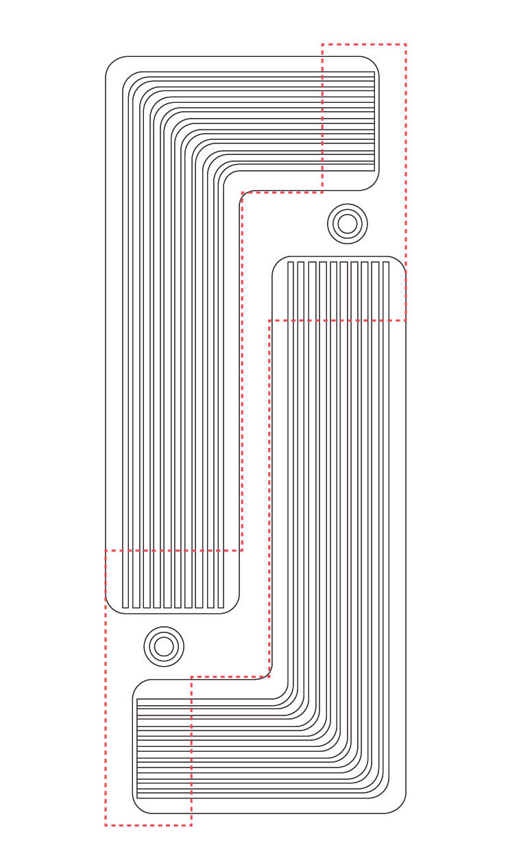
Marking lines are added at the head and tail welding positions of the "L shaped" circuit and the head and tail welding positions of the inverted "L shaped" circuit. The marking lines are roughly the same in shape and size as the reinforcement board to be attached to the flexible printed circuit (as shown in the yellow mark on the back of Figure 3). The marking lines of the " L shaped" circuit and the inverted " L shaped" circuit on the same circuit arrangement area are connected to form a closed pattern (as shown in the red dotted line mark in Figure 2), which is a detection pattern for quickly checking whether the sample flexible printed circuit stiffener or double-sided adhesive is offset.

The line width of the marking line is 0.6mm to meet the tolerance of the stiffener ±0.3mm. In this way, as long as the edge of the stiffener is within the line width, the size of the attached product meets the requirements. At present, the tolerance of flex PCB stiffener or double-sided adhesive in the industry is ±0.3mm. For this reason, the line width of the quick inspection mark line is designed to be 0.6mm. There are also some special specifications. For stiffener or double-sided adhesive with special specifications, the line width must be redesigned according to the drawing requirements when designing the film, but the design principle is the same.
Σχόλια