Multi layer Flex PCB

A multi-layer flex PCB is a circuit board made of alternating single-sided or double-sided circuits. It combines the flexibility of a flex PCB with the high-density circuit capabilities of a multi-layer PCB. The layers are connected by conductive holes (common conductive holes include through holes, blind holes, and buried holes).
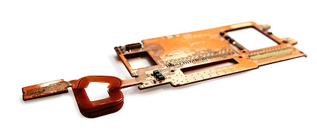
During the entire production process, multiple layers can be laminated together continuously or discontinuously. As shown in our picture, there are soft parts and rigid parts on a multi-layer flexible PCB, which are all determined by your design.
Stack-up
Multilayer flexible circuit boards can be composed of several single sided flex PCBs, several double sided flex PCBs, or a mixture of single layers and double layers. When we say how many layers a circuit board has, we are referring to the number of conductive layers. So below is the stackup diagram for a 4 layers flex PCB.

Stack-up of multi layer flex PCB
Multilayer Flexible Circuit Board
Technical Specifications
Layer Count Range:
Standard multilayer flex PCB: 2-12 layers (customizable up to 16 layers for special requirements)
Hybrid structures ( Rigid-Flex PCBs ): Composite design of flexible layers + rigid layers

Circuit Parameters:
Minimum line width/spacing: 0.05mm/0.05mm (using laser direct imaging technology)
Minimum hole diameter (mechanical drilling): 0.1mm (blind/buried vias require laser drilling, with a minimum hole diameter of 0.05mm)
Material Specifications:
Substrate: Polyimide (PI) film, thickness ranging from 12.5μm to 50μm
Copper foil thickness: 1/3 oz (12μm) to 2 oz (70μm)
Coverlay: PI-based material, thickness ranging from 12.5μm to 25μm
Electrical Performance:
Impedance control: ±10% tolerance (±5% for high-frequency applications)
Dielectric strength: 500V~3kV (adjusted based on insulation layer thickness)
Design Guidelines of Multilayers Flex PCB
Bend Design Optimization:
Dynamic bending: Bend radius ≥ 10 times the board thickness (e.g., for a 0.2mm thick board, the bend radius should be ≥ 2mm)
Static bending: Bend radius ≥ 6 times the board thickness
Avoid placing vias or pads in the bending area to reduce stress concentration
Layer Stackup Symmetry:
Multilayer circuit boards should maintain symmetrical stacking
(e.g., a 4-layer structure: FCCL + Adhesive + Core + Adhesive + FCCL) to minimize warpage risks.
Routing Considerations:
Adjacent layers should have orthogonal trace designs (to minimize crosstalk), and critical signal traces should be shielded with ground layers.
Thermal Management:
For high-power areas, use locally thickened copper foil (2 oz) or add thermal conductive adhesive.
Multi-layer Flex PCB Benefits
-
High circuit density: Suitable for complex systems that require high circuit integration.
-
Stronger electrical performance: The multilayer structure of a flexible circuit can reduce electromagnetic interference (EMI) and crosstalk and provide stable signal transmission.
-
Smaller size: Since circuits can be done on multiple layers, the product size can be reduced, which is suitable for miniaturized design.
-
Strong reliability: Multilayer flex circuits are suitable for harsh environmental conditions, such as aerospace and automotive electronics.
Applications
Multilayer flex PCB are an effective solution when faced with the following design challenges: unavoidable crossovers, specific impedance requirements, crosstalk elimination, additional shielding, and high component density.
-
Aerospace: Due to its excellent performance and reliability, multilayer flex PCB is suitable for aerospace equipment and instruments.
-
High-frequency communication: Such as in high-frequency circuits like 5G base stations and radar systems.
-
Industrial control: Works well in factory automation and robot control systems, etc.
-
Medical equipment: Perfect for modern medical devices that need compact and trustworthy circuits.
Advanced Features
-
High-speed signal transmission: Multilayer flex PCB is suitable for high-speed data transmission applications, reducing delays and signal attenuation.
-
High-temperature resistance: Multilayer for flexible circuit design provides better thermal management capabilities and can withstand higher operating temperatures.
-
Precise interlayer connection: Use microvia or blind hole technology to achieve efficient connection between different layers and improve overall performance.
Manufacturing Process
-
Material Preparation: Laser cutting of PI substrate, cleaning of copper foil surface to remove oxides.
-
Inner Layer Pattern Formation: Dry film lamination → Exposure → Development → Etching → Stripping (trace width tolerance ±30μm).
-
Lamination: Hot press process (180-200℃, pressure 15-30kg/cm²) using acrylic or epoxy adhesive for interlayer bonding.
-
Drilling & Hole Metallization: Mechanical drilling (hole diameter ≥0.1mm) or laser drilling (hole diameter ≥0.05mm) → Electroless copper plating → Full-board electroplating (minimum hole copper thickness ≥6μm).
-
Outer Layer Pattern & Surface Treatment: Secondary etching → Coverlay opening → ENIG/OSP/Electroplated gold (depending on soldering requirements).
-
Final Inspection & Testing: 100% electrical connectivity test → Automated Optical Inspection (AOI) (defect rate <0.1%) → Impedance testing (using a network analyzer).
Quality Control Measures
Process Control:
Each batch undergoes DSC (thermal analysis) and DMA (mechanical performance testing).
X-ray inspection of layer alignment after lamination (tolerance <25μm).
Reliability Testing:
Bending life test (dynamic bending 100,000 times without fracture, meeting IPC-6013 standards).
High-temperature, high-humidity test (85℃/85%RH for 1000 hours) ensuring insulation resistance >1GΩ.
FAQ
Q1: How to choose the number of layers and materials?
The complexity of the signal determines the number of layers (e.g., a 4-layer board is suitable for general control circuits, while 8 layers or more are used for high-speed signals).
For high-frequency applications, choose low Dk/Df PI substrates (e.g., DuPont Pyralux AP).
Q2: How to prevent flexible boards from breaking during installation?
Use stiffeners (FR4, PI, Aluminum, etc.) in fixed areas, and design gradual width transitions in transition areas to avoid right-angle traces.
Q3: What factors affect lead time and cost?
Lead time: Standard 4-layer boards take 2-3 weeks, while complex rigid-flex boards take 4-6 weeks.
Cost drivers: Number of laser-drilled holes, special surface treatments (e.g., immersion silver), proportion of impedance-controlled layers.


Discover top-quality flex PCBs at Flex Plus. Our advanced flexible PCBs are designed for durability and high performance.
Contact us today for custom flex circuit solutions that meet your exact specifications.